
Friday, 19 April 2024
New or improved technologies, such as artificial intelligence, 5G cellular communications, and the Internet-of-Things, are expected to bring revolutionary changes in society. But for that to happen, high-performance system-on-a-chip (SoC)—a type of integrated circuit—devices are indispensable. A core building block of SoC devices is the phase-locked loop (PLL), a circuit that synchronizes with the frequency of a reference oscillation and outputs a signal with the same or higher frequency. PLLs generate 'clocking signals', whose oscillations act as a metronome that provides a precise timing reference for the harmonious operation of digital devices.
For high performance SoC devices to be realized, fabrication processes for semiconductor electronics must become more sophisticated. The smaller the area to implement digital circuitry is, the better the performance of the device. Manufacturers have been racing to develop increasingly smaller semiconductors. 7 nm semiconductors (a massive improvement over their 10 nm predecessor) are already in production, and methods to build 5 nm ones are now being looked at.
However, in this endeavor stands a major bottleneck. Existing PLLs require analog components, which are generally bulky and have designs that are difficult to scale down.
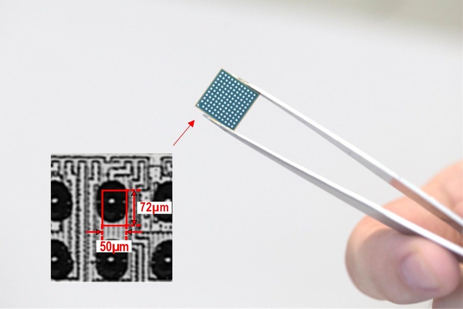
Scientists at Tokyo Tech and Socionext Inc., led by Prof. Kenichi Okada, have addressed this issue by implementing a 'synthesizable' fractional-N PLL, which only requires digital logic gates, and no bulky analog components, making it easy to adopt in conventional miniaturized integrated circuits.
Okada and team used several techniques to decrease the required area, power consumption and jitter—unwanted time fluctuations when transmitting digital signals—of their synthesizable PLLs. To decrease area, they employed a ring oscillator, a compact oscillator that can be easily scaled down. To suppress jitter, they reduced the phase noise—random fluctuations in a signal—of this ring oscillator, using 'injection locking'—the process of synchronizing an oscillator with an external signal whose frequency (or multiple of it) is close to that of the oscillator—over a wide range of frequencies. The lower phase noise, in turn, reduced power consumption.
The design of this synthesizable PLL beats that of all other current state-of-the-art PLLs in many important aspects. It achieves the best jitter performance with the lowest power consumption and smallest area (as can be seen in Figure 1). "The core area is 0.0036 mm2, and the whole PLL is implemented as one layout with a single power supply," remarks Okada. Further, it can be built using standard digital design tools, allowing for its rapid, low-effort, and low-cost production, making it commercially viable.
This synthesizable PLL can be easily integrated into the design of all-digital SoCs, and is commercially viable, making it valuable for developing the much sought after 5 nm semiconductor for cutting-edge applications including artificial intelligence, internet of things and many others, where high performance and low power consumption would be the critical requirements. But the contributions of this research go beyond these possibilities. "Our work demonstrates the potential of synthesizable circuits. With the design methodology employed here, other building blocks of SoCs, such as data converters, power management circuits, and wireless transceivers, could be made synthesizable as well. This would greatly boost design productivity and considerably reduce design efforts," explains Okada. Tokyo Tech and Socionext will continue their collaboration in this filed to advance the miniaturization of electronic devices, enabling the realization of newer-generation technologies.
This research work was conducted in cooperation with TeraPixel Technologies Inc.

Meeta develops credible content about various markets based on deep research, opinions from experts and inputs from industry leaders. As the managing editor at Smart Market News, she assures that every piece of news and article adds to the knowledge of decision makers. An avid bike rider, Meeta, is a postgraduate from Indian Institute of Journalism and New Media (IIJNM) Bangalore, where her specialization was Business Journalism. She carries experience from mainstream print media including The Times Group and Sakal Media Group.

Smarter Decisions with Smart News
Smart Market News is committed to getting its readers the latest updates and insights on industries that help in making “smarter” business decisions. With insights and inputs from corporate decision makers, we bring you the stories of adopting innovative solutions and strategies that have been changing the world. Our editorial insights on products, solutions, companies, and adoption of best practices not only help in understanding the markets better, but also prove to be a complete package for your information needs.


 Even though China is trying, Europe to Continue its Dominance Rubber-Tyred Gantr..
  New Ford CEO Farley eyes expansion into tech fields